- 您現在的位置:買賣IC網 > PDF目錄371062 > MC74F85 (Motorola, Inc.) 4-BIT MAGNITUDE COMPARATOR PDF資料下載
參數資料
| 型號: | MC74F85 |
| 廠商: | Motorola, Inc. |
| 英文描述: | 4-BIT MAGNITUDE COMPARATOR |
| 中文描述: | 4位數值比較 |
| 文件頁數: | 4/4頁 |
| 文件大小: | 90K |
| 代理商: | MC74F85 |
4-39
FAST AND LS TTL DATA
MC54/74F85
AC ELECTRICAL CHARACTERISTICS
54/74F
54F
74F
TA = +25
°
C
VCC = +5.0 V
CL = 50 pF
TA = –55
°
C to +125
°
C
VCC = 5.0 V
±
10%
CL = 50 pF
TA = 0
°
C to + 70
°
C
VCC = 5.0 V
±
10%
CL = 50 pF
Symbol
Parameter
Min
Max
Min
Max
Min
Max
Unit
tPLH
tPHL
tPLH
tPHL
tPLH
A or B Input to
6.0
11
5.5
14
5.5
13
ns
A < B, A > B Output
6.0
14
5.5
16.5
5.5
15.5
A or B Input to
5.5
11.5
5.0
15
5.0
14
ns
A = B Output
7.0
14
6.5
15.5
6.5
14.5
IA<B and IA=B Input
3.0
7.5
2.5
10
2.5
9.0
ns
tPHL
tPLH
tPHL
tPLH
tPHL
to A>B Output
3.0
9.0
2.5
11
2.5
10
IA=B Input to
A = B Output
2.5
7.0
2.0
10
2.0
9.0
ns
3.5
10
2.5
13
2.5
12
IA>B and IA=B Input
to A<B Output
3.0
8.0
3.0
10.5
3.0
9.5
ns
3.0
9.0
2.0
10.5
2.0
9.5
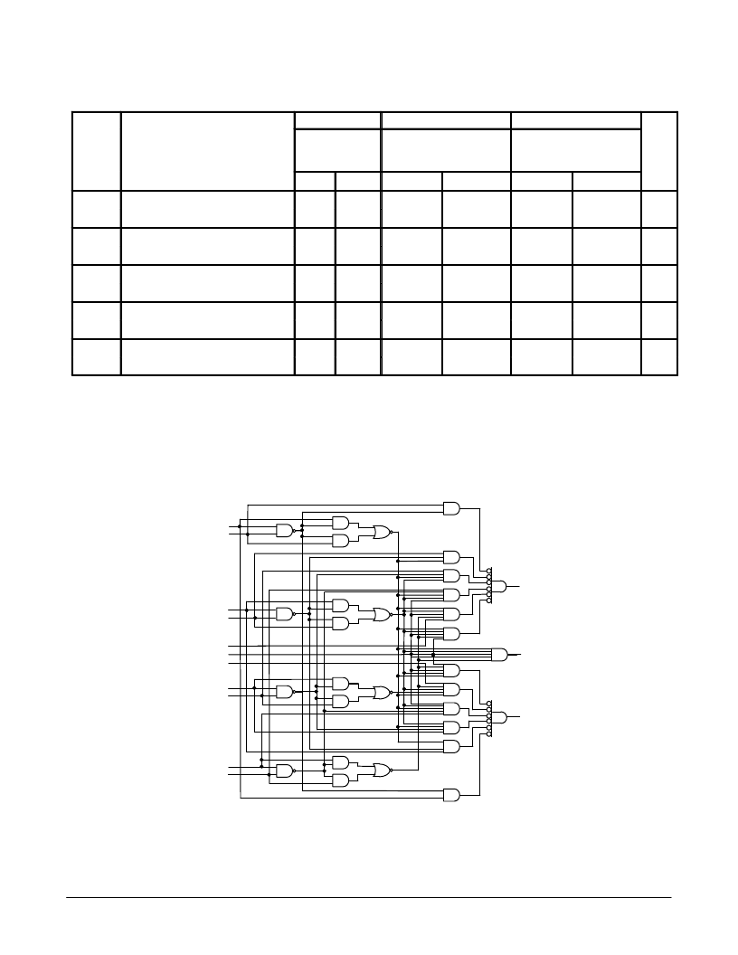
The expansion inputs IA>B, IA=B, and IA<B are the least sig-
nificant bit positions. When used for series expansion, the
A>B, A=B, and A<B outputs of the least significant word are
connected to the corresponding IA>B, IA=B, and IA<B nputs of
the next higher stage. Stages can be added in this manner
to any length, but a propagation delay penalty of about 15 ns
is added with each additional stage. For proper operation the
expansion inputs of the least significant word should be tied
as follows: IA>B = LOW, IA=B = HIGH, and IA<B = LOW.
IA < B
IA = B
IA > B
NOTE:
This diagram is provided only for the understanding of logic operations and should not be used
to estimate propagation delays.
Figure 2. Logic Diagram
(15)
(1)
A3
B3
A2
B2
(13)
(14)
(2)
(3)
A1
B1
(12)
(11)
(4)
(5)
(6)
(7)
A > B
A = B
A < B
A0
B0
(10)
(9)
相關PDF資料 |
PDF描述 |
|---|---|
| MC74F85D | 4-BIT MAGNITUDE COMPARATOR FAST SCHOTTKY TTL |
| MC74F85J | 4-BIT MAGNITUDE COMPARATOR FAST SCHOTTKY TTL |
| MC74F85N | 4-BIT MAGNITUDE COMPARATOR FAST SCHOTTKY TTL |
| MC74F86 | QUAD 2-INPUT EXCLUSIVE-OR GATE |
| MC74F86D | QUAD 2-INPUT EXCLUSIVE-OR GATE FAST SCHOTTKY TTL |
相關代理商/技術參數 |
參數描述 |
|---|---|
| MC74F85M | 制造商:Rochester Electronics LLC 功能描述:- Bulk |
| MC74F85N | 制造商:Rochester Electronics LLC 功能描述:- Bulk 制造商:Motorola Inc 功能描述: 制造商:ON Semiconductor 功能描述: |
| MC74F86D | 制造商:Motorola Inc 功能描述: |
| MC74F86MR1 | 制造商:ON Semiconductor 功能描述: |
| MC74F86N | 制造商:ON Semiconductor 功能描述: |
發布緊急采購,3分鐘左右您將得到回復。