- 您現在的位置:買賣IC網 > PDF目錄371076 > MC88921 (Motorola, Inc.) LOW SKEW CMOS PLL CLOCK DRIVER With Power-Down/ Power-Up Feature PDF資料下載
參數資料
| 型號: | MC88921 |
| 廠商: | Motorola, Inc. |
| 英文描述: | LOW SKEW CMOS PLL CLOCK DRIVER With Power-Down/ Power-Up Feature |
| 中文描述: | 低偏移的CMOS PLL時鐘驅動器,掉電/啟動功能 |
| 文件頁數: | 2/10頁 |
| 文件大小: | 106K |
| 代理商: | MC88921 |
MC88921
MOTOROLA
TIMING SOLUTIONS
BR1333 — REV 5
2
19
20
18
17
16
15
14
13
12
11
2
1
3
4
5
6
7
8
9
10
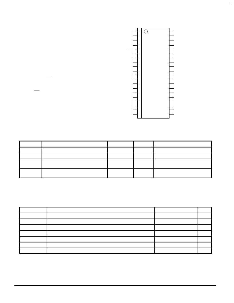
Pinout: 20–Lead Wide SOIC Package
(Top View)
GND
Q3
2X_Q
VCC
Q/2
MR
VCC
PLL_EN
Q2
VCC(AN)
GND
RC1
LOCK
GND(AN)
FBSEL
SYNC
Q1
GND
VCC
Q0
Power–Down Mode Functionality
The MC88921 has a special feature
designed in to allow the processor clock
inputs to be reset for total processor
power–down, and then to return to
phase–locked operation very quickly when
the processor is powered–up again.
The MR pin resets outputs 2X_Q, Q0
and Q1 only leaving the other outputs
operational for other system activity. When
MR is negated, all outputs will be operating
normally within 3 clock cycles.
CAPACITANCE AND POWER SPECIFICATIONS
Symbol
Parameter
Value Typ
Unit
Test Conditions
CIN
Input Capacitance
4.5
pF
VCC = 5.0V
CPD
Power Dissipation Capacitance
40
pF
VCC = 5.0V
PD1
Power Dissipation at 33MHz With 50
Thevenin Termination
15mW/Output
90mW/Device
mW
VCC = 5.0V
T = 25
°
C
PD2
Power Dissipation at 33MHz With 50
Parallel Termination to GND
37.5mW/Output
225mW/Device
mW
VCC = 5.0V
T = 25
°
C
MAXIMUM RATINGS*
Symbol
Parameter
Limits
Unit
VCC, AVCC
Vin
Vout
Iin
Iout
ICC
Tstg
DC Supply Voltage Referenced to GND
–0.5 to 7.0
V
DC Input Voltage (Referenced to GND)
–0.5 to VCC +0.5
–0.5 to VCC +0.5
±
20
V
DC Output Voltage (Referenced to GND)
V
DC Input Current, Per Pin
mA
DC Output Sink/Source Current, Per Pin
±
50
mA
DC VCC or GND Current Per Output Pin
Storage Temperature
±
50
mA
–65 to +150
°
C
* Maximum Ratings are those values beyond which damage to the device may occur. Functional operation should be restricted to the
Recommended Operating Conditions.
相關PDF資料 |
PDF描述 |
|---|---|
| MC88LV915 | LOW SKEW CMOS PLL CLOCK DRIVER |
| MC88LV915T | LOW SKEW CMOS PLL CLOCK DRIVER |
| MC88LV926 | LOW SKEW CMOS PLL 68060 CLOCK DRIVER |
| MC88LV926DW | LOW SKEW CMOS PLL 68060 CLOCK DRIVER |
| MC88PL117 | CMOS PLL CLOCK DRIVER |
相關代理商/技術參數 |
參數描述 |
|---|---|
| MC88921DW | 制造商:MOTOROLA 制造商全稱:Motorola, Inc 功能描述:LOW SKEW CMOS PLL CLOCK DRIVER With Power-Down/ Power-Up Feature |
| MC889AL | 制造商:Rochester Electronics LLC 功能描述:- Bulk |
| MC889AP | 制造商:Motorola Inc 功能描述: 制造商:MOTOROLA 功能描述: |
| MC88A | 制造商:未知廠家 制造商全稱:未知廠家 功能描述:8 TUNES 8 KEY WITH SCAN KEY |
| MC88B/IVY | 制造商:TELEPHONE EQUIPMENT 功能描述:THREE COUPLER 8P8C |
發布緊急采購,3分鐘左右您將得到回復。