- 您現在的位置:買賣IC網 > PDF目錄361231 > Q67060-S6111-A3 (INFINEON TECHNOLOGIES AG) Smart High-Side Power Switch One Channel: 38mз Status Feedback PDF資料下載
參數資料
| 型號: | Q67060-S6111-A3 |
| 廠商: | INFINEON TECHNOLOGIES AG |
| 英文描述: | Smart High-Side Power Switch One Channel: 38mз Status Feedback |
| 中文描述: | 智能高側電源開關一個頻道:38mз狀態反饋 |
| 文件頁數: | 8/12頁 |
| 文件大小: | 261K |
| 代理商: | Q67060-S6111-A3 |
BTS436L2
Semiconductor Group
Page 8
2003-Oct-01
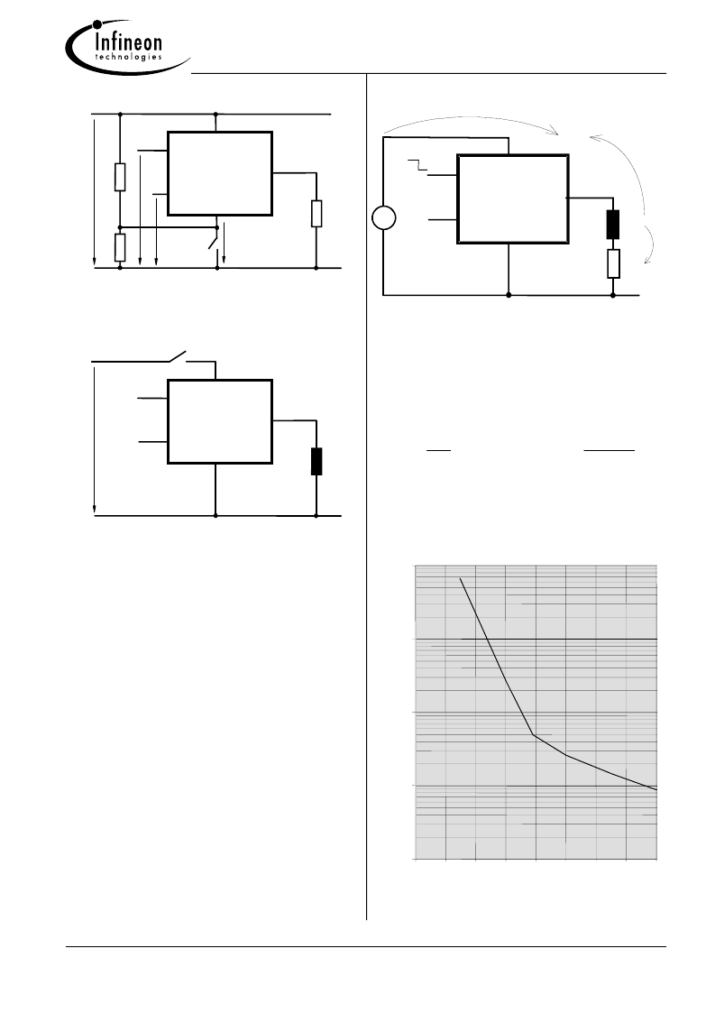
GND disconnect with GND pull up
PROFET
V
IN
ST
OUT
GND
bb
Vbb
1
2
4
3
5
VGND
VINVST
Any kind of load. If V
GND >
V
IN
-
V
IN(T+)
device stays off
Due to V
GND
>0, no V
ST
= low signal available.
V
bb
disconnect with energized inductive
load
PROFET
V
IN
ST
OUT
GND
bb
Vbb
1
2
4
3
5
high
For inductive load currents up to the limits defined by ZL
(max. ratings and diagram on page 8) each switch is
protected against loss of Vbb.
Consider at your PCB layout that in the case of Vbb dis-
connection with energized inductive load all the load current
flows through the GND connection.
Inductive Load switch-off energy
dissipation
E
bb
PROFET
V
IN
ST
OUT
GND
bb
=
E
E
EAS
L
R
ELoad
L
R
L
{
Z
L
Energy stored in load inductance:
E
L
=
1/2
·
L
·
I
2
L
While demagnetizing load inductance, the energy
dissipated in PROFET is
E
AS
= E
bb
+ E
L
- E
R
=
V
ON(CL)
·
i
L
(t) dt,
with an approximate solution for R
L
>
0
:
E
AS
= I
L
·
L
2
·
R
L
·
(
V
bb
+
|V
OUT(CL)
|)
·
ln
(1+
I
L
·
R
L
|V
OUT(CL)
| )
Maximum allowable load inductance for
a single switch off
L = f (I
L
);
T
j,start
=
150°C,
T
C
=
150°C const.,
V
bb
=
12
V,
R
L
=
0
Z
L
[mH]
1000
1
10
100
0
2
4
6
10
12
14
16
18
0.1
I
L [A]
相關PDF資料 |
PDF描述 |
|---|---|
| Q67060-S6111-A4 | Smart High-Side Power Switch One Channel: 38mз Status Feedback |
| Q67060-S6112-A2 | High Speed CMOS Logic Dual 4-Input NOR Gates 14-SO -55 to 125 |
| Q67060-S6112-A3 | High Speed CMOS Logic Dual 4-Input NOR Gates 14-SO -55 to 125 |
| Q67060-S6112-A4 | High Speed CMOS Logic Dual 4-Input NOR Gates 14-SO -55 to 125 |
| Q67060-S6201-A2 | High Speed CMOS Logic Dual 4-Input NOR Gates 14-TSSOP -55 to 125 |
相關代理商/技術參數 |
參數描述 |
|---|---|
| Q67060-S6111-A4 | 制造商:INFINEON 制造商全稱:Infineon Technologies AG 功能描述:Smart High-Side Power Switch One Channel: 38mз Status Feedback |
| Q67060-S6112-A2 | 制造商:INFINEON 制造商全稱:Infineon Technologies AG 功能描述:Smart Highside Power Switch One Channel: 20mз |
| Q67060-S6112-A3 | 制造商:INFINEON 制造商全稱:Infineon Technologies AG 功能描述:Smart Highside Power Switch One Channel: 20mз |
| Q67060-S6112-A4 | 制造商:INFINEON 制造商全稱:Infineon Technologies AG 功能描述:Smart Highside Power Switch One Channel: 20mз |
| Q67060-S6118 | 制造商:INFINEON 制造商全稱:Infineon Technologies AG 功能描述:Smart Highside Power Switch One Channel: 20mз Status Feedback |
發布緊急采購,3分鐘左右您將得到回復。