- 您現在的位置:買賣IC網 > PDF目錄371046 > MC68B912B32 (Motorola, Inc.) 2.5V 100ppm/Degrees C, 50uA in SOT23-3 Series (Bandgap) Voltage Reference 3-SOT-23 -40 to 125 PDF資料下載
參數資料
| 型號: | MC68B912B32 |
| 廠商: | Motorola, Inc. |
| 英文描述: | 2.5V 100ppm/Degrees C, 50uA in SOT23-3 Series (Bandgap) Voltage Reference 3-SOT-23 -40 to 125 |
| 中文描述: | 16位微控制器 |
| 文件頁數: | 10/128頁 |
| 文件大小: | 748K |
| 代理商: | MC68B912B32 |
第1頁第2頁第3頁第4頁第5頁第6頁第7頁第8頁第9頁當前第10頁第11頁第12頁第13頁第14頁第15頁第16頁第17頁第18頁第19頁第20頁第21頁第22頁第23頁第24頁第25頁第26頁第27頁第28頁第29頁第30頁第31頁第32頁第33頁第34頁第35頁第36頁第37頁第38頁第39頁第40頁第41頁第42頁第43頁第44頁第45頁第46頁第47頁第48頁第49頁第50頁第51頁第52頁第53頁第54頁第55頁第56頁第57頁第58頁第59頁第60頁第61頁第62頁第63頁第64頁第65頁第66頁第67頁第68頁第69頁第70頁第71頁第72頁第73頁第74頁第75頁第76頁第77頁第78頁第79頁第80頁第81頁第82頁第83頁第84頁第85頁第86頁第87頁第88頁第89頁第90頁第91頁第92頁第93頁第94頁第95頁第96頁第97頁第98頁第99頁第100頁第101頁第102頁第103頁第104頁第105頁第106頁第107頁第108頁第109頁第110頁第111頁第112頁第113頁第114頁第115頁第116頁第117頁第118頁第119頁第120頁第121頁第122頁第123頁第124頁第125頁第126頁第127頁第128頁
MOTOROLA
10
MC68HC912B32
MC68HC912B32TS/D
3.2 Power Supply Pins
MC68HC912B32 power and ground pins are described below and summarized in
Table 4
.
3.2.1 Internal Power (V
DD
) and Ground (V
SS
)
Power is supplied to the MCU through V
DD
and V
SS
. Because fast signal transitions place high, short-
duration current demands on the power supply, use bypass capacitors with high-frequency character-
istics and place them as close to the MCU as possible. Bypass requirements depend on how heavily
the MCU pins are loaded.
3.2.2 External Power (V
DDX
)
and Ground (V
SSX
)
External power and ground for I/O drivers. Because fast signal transitions place high, short-duration cur-
rent demands on the power supply, use bypass capacitors with high-frequency characteristics and
place them as close to the MCU as possible. Bypass requirements depend on how heavily the MCU
pins are loaded.
3.2.3 V
DDA
, V
SSA
Provides operating voltage and ground for the analog-to-digital converter. This allows the supply volt-
age to the A/D to be bypassed independently.
3.2.4 Analog-to-Digital Reference Voltages (V
RH
, V
RL
)
3.2.5 V
FP
Flash EEPROM programming voltage and supply voltage during normal operation.
3.2.6 V
PP
High voltage supply to EEPROM. Used to monitor charge pump output and testing. Not intended for
general applications use.
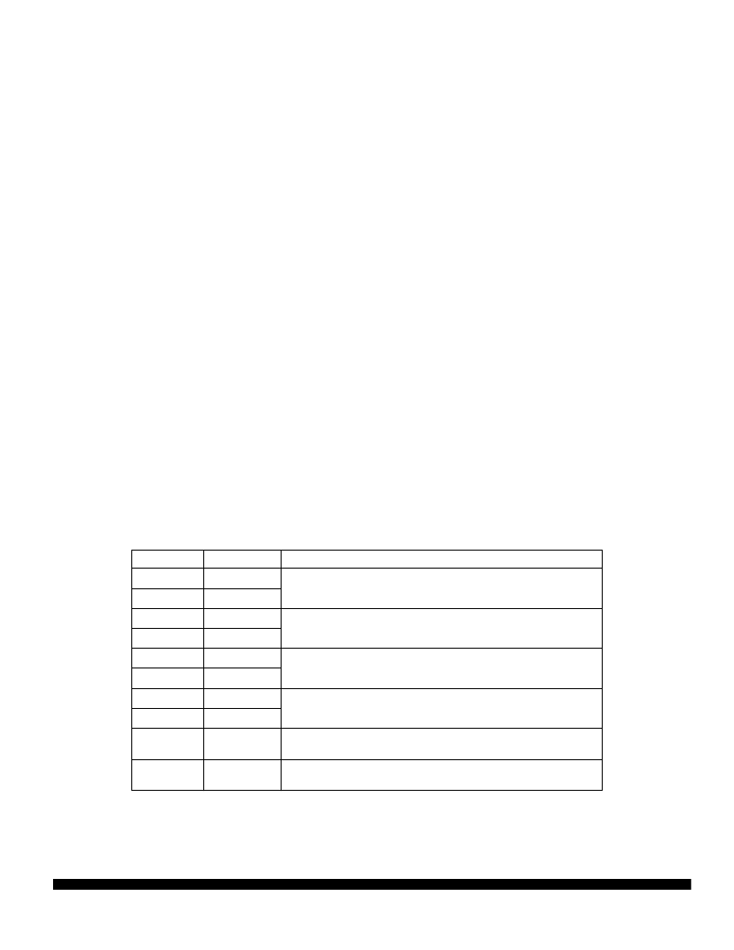
Table 4 MC68HC912B32 Power and Ground Connection Summary
Mnemonic
V
DD
V
SS
V
DDX
V
SSX
V
DDA
V
SSA
V
RH
V
RL
Pin Number
Description
10, 47
Internal power and ground.
11, 48
31, 78
External power and ground, supply to pin drivers.
30, 77
59
Operating voltage and ground for the analog-to-digital converter,
allows the supply voltage to the A/D to be bypassed independently.
60
49
Reference voltages for the analog-to-digital converter.
50
V
FP
69
Programming voltage for the Flash EEPROM and required supply
for normal operation.
High voltage supply to EEPROM used for test purposes only in
special modes.
V
PP
37
相關PDF資料 |
PDF描述 |
|---|---|
| MC68C912B32FU8 | 16-Bit Microcontroller |
| MC68B912B32FU8 | 16-Bit Microcontroller |
| MC68C912B32CFU8 | 16-Bit Microcontroller |
| MC68CK338 | Highly Integrated, Low-Power, 32-Bit Microcontroller |
| MC68EC060 | 32-Bit Microprocessors.(32位微處理器) |
相關代理商/技術參數 |
參數描述 |
|---|---|
| MC68B912B32FU8 | 制造商:MOTOROLA 制造商全稱:Motorola, Inc 功能描述:16-Bit Microcontroller |
| MC68BOOL | 制造商:MOTOROLA 制造商全稱:Motorola, Inc 功能描述:8-BIT MICROPROCESSING UNIT (MPU) |
| MC68BOOP | 制造商:MOTOROLA 制造商全稱:Motorola, Inc 功能描述:8-BIT MICROPROCESSING UNIT (MPU) |
| MC68BOOS | 制造商:MOTOROLA 制造商全稱:Motorola, Inc 功能描述:8-BIT MICROPROCESSING UNIT (MPU) |
| MC68C812A4 | 制造商:FREESCALE 制造商全稱:Freescale Semiconductor, Inc 功能描述:Technical Supplement MC68C812A4 3.3V Electrical Characteristics |
發布緊急采購,3分鐘左右您將得到回復。